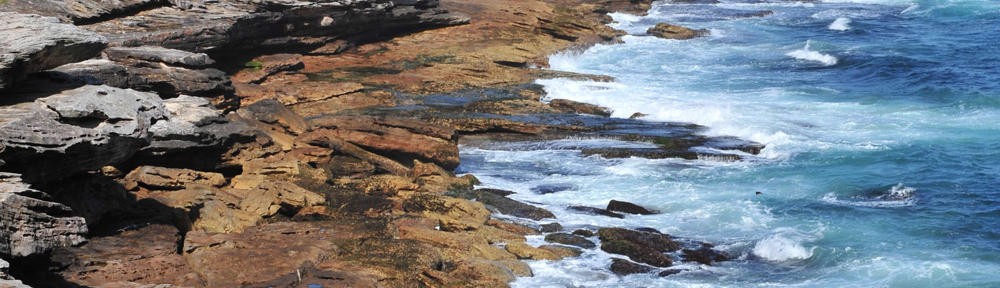
55Ge0.45 quantum well and a 100-nm intrinsic Si capping layer [20]. The constructions of three types of NRs are given in Figure 1a, together with the scanning electron microscopy (SEM) image of NR2. The SEM images of NR1 and NR3 are similar to that of NR2, except the length of NR1 is smaller than the other two. Figure 1b gives an experimental schematic diagram of EFM measurements on single Si NRs combined with laser irradiation. The phase shift vs. voltage (ΔΦ − V EFM) curves are measured at a lift height on single NRs with SCM-PIT tips. Laser (405 nm) with adjustable power intensity is focused onto the substrate through a 400-μm fiber,
with a spot of about 1 mm2 at the area beneath the AFM tip. All measurements are operated in a nitrogen flow gas for a stable measurement. Figure 1 Constructions of NRs and schematic diagram of EFM measurements. (a) SEM image of NR2, together with the
constructions of NR1, NR2, and NR3. check details (b) Schematic diagram of EFM measurements on single Si NRs combined with a 405-nm laser irradiation. Results and discussions The ΔΦ − V EFM curves measured at a lift height of 140 nm on three samples under different laser intensities BI 2536 price are shown in Figure 2 as the scattered dots. It can be seen that the curves shift to the negative direction with the laser intensity, and the shift varies with the type of the NRs. In previous literatures, the relation between phase shift and electrostatic force has been established, where the tip-sample system is simply treated as plane capacitor [21–23]. When a bias is applied between the tip and the sample, the capacitive electrostatic force gradient would cause a phase shift.
If there are charges trapped in the sample, additional phase shift induced by the coulombic force is generated. Therefore, at the lifted pass where the Van der Waals force can be ignored, the force on the tip can be written as [11, 24, 25]: (1) Figure 2 ΔΦ − V EFM curves measured at different laser intensities for NR1 (a), NR2 (b), and NR3 (c). The experimental data are plotted with scattered dots, and the fitting results are given with lines. A fitting example of NR1 without laser is presented in the inset of (a). Where C, V EFM, and V CPD are the capacitance, applied DC Cobimetinib nmr voltage, and contact potential difference (CPD) between the tip and sample, respectively. Q s is the amount of charges trapped in the beneath NR, and z is the distance between the trapped charges in NR and image charges in tip. The phase shift detected by EFM is proportional to the gradient of the force, which is as follows: (2) where Q is the quality factor and k is the spring constant of the probe. From Equation 2, it can be seen, without charges trapped in Si NRs, that the EFM phase shift should be equal to zero at V EFM = V CPD. In other words, the minimum point of the ΔΦ − V EFM curve should be located at zero.